Product Overview

Single Photon Detector

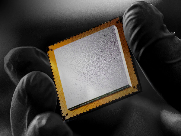
Superconducting-class performance from a semiconductor detector, cooled by a compact TEC instead of a cryostat.

s
s
g
u
z
d
d
g
s
r
Performance
Every photon, accounted for.
Over 90% absorption from 900 to 1500 nm, timing jitter under 50 picoseconds, and a TEC-cooled package that runs at 200 K with no cryogenics.
>75%
Peak detection efficiency
<50 ps
Timing jitter
200 K
TEC-cooled, no cryogenics
MeasuredCalculated
100%75%50%25%0% 900110013001500 Wavelength (nm) Absorption efficiency
Abstract digital green light beams and grid patterns creating a futuristic symmetrical tunnel effect on a black background.
The photon problem
When every photon carries information, detection becomes the bottleneck.
Superconducting nanowire detectors set the performance bar, but they need cryogenic infrastructure that keeps them in the lab. Conventional semiconductor detectors are portable, but give up detection efficiency or timing resolution. QuantumCore closes that gap.
Arrow right icon
Engineered photon by photon. At the heart of the detector is a semiconductor metasurface: an array of nanostructures whose shape and geometry are tuned to absorb light and control where it lands.
01
Engineer the metasurface
A semiconductor wafer is patterned into a precisely designed array of nanostructures, each pillar sized and shaped to interact with light at the subwavelength scale.
02
Absorb near-perfectly
The metasurface geometry suppresses reflection and guides incident light into the active region, with near-unity absorption measured across 900 nm to 1600 nm.
03
Control where light lands
The metasurface localizes absorption to a well-defined region. That tight control delivers timing resolution beyond the limits of conventional semiconductor detectors.
04
Trigger the avalanche
An absorbed photon starts an avalanche of charge carriers in the InGaAs/InP diode, amplified into a crisp electrical pulse of 1 V or more on a standard SMA output.
05
Cool with a TEC, not a cryostat
A compact thermoelectric cooler holds the hermetically sealed package at 200 K to suppress dark counts. No cryostat, no helium, no bulky infrastructure.
A small footprint, without cryogenic cooling. The detector sits in a hermetically sealed, TEC-cooled package inside a compact module, ready for the lab, the field, or orbit.
Free-space coupling, with optional FC/PC or FC/APC fiber.
Active area from 10 to 50 µm in diameter.
Output pulse of 1 V or more on a standard SMA interface.
Hermetic package
The devices are cooled with a TEC in a hermetically sealed package to 200 K. No cryogenics required.
Placeholder image
Placeholder image
Key specifications
Target specifications
Core technology
InGaAs/InP single-photon avalanche diodes with patterned metasurfaces for near-unity absorption efficiency in the active region.
Operating wavelength
900 nm – 1700 nm
Peak detection efficiency¹
> 75%
Timing jitter²
< 50 ps
Dark count rate³
< 1000 Hz
Optical coupling
Free space (fiber coupling optional: FC/PC or FC/APC)
Active area
Ø 10–50 µm diameter
Output pulse height
≥ 1 V
Output pulse interface
SMA
¹ The wavelength corresponding to the peak detection efficiency depends on the geometry of the nanostructured array. The target specification is based on the measured absorption efficiency and the calculated impact ionization probability required to initiate the avalanche process in our device design.
² 20 ps timing jitter measured in an InP nanostructure array. S. Gibson et al., Nature Nanotechnology 14 (5), 473–479 (2019).
³ To be determined. A dark count rate of < 100 Hz was measured in InGaAs/GaAs nanostructure arrays at 125 K. A.C. Farrell et al., Nano Letters 19 (1), 582–590 (2018).
Arrow right icon
Placeholder image
Built for every scenario where a single photon carries the answer. From quantum networks to live-cell imaging, high-efficiency detection unlocks measurements that were out of reach.
Quantum computing
01
Photonic quantum computers need thousands of high-efficiency detectors working in parallel to read out qubit states. A semiconductor architecture removes the cryogenic bottleneck.
Photonic qubit readout
Large-area detector arrays
Photonic circuit integration
Quantum communication
02
Every extra detected photon raises the secure key rate of a QKD link, on the ground or in orbit, without the mass and power cost of cryogenic coolers.
QKD receivers
Satellite links
Portable field deployment
Biological imaging
03
Photon-starved samples can't tolerate bright illumination. A detector that registers almost every photon turns a faint biological signal into a usable image.
Fluorescence imaging
Deep-tissue imaging
Low-light microscopy
Networks and sensing
04
Precise single-photon detection confirms entanglement between remote network nodes and enables new sensing in defence, aerospace and semiconductor failure analysis.
Entanglement distribution
CMOS failure analysis
Quantum sensing
Data sheet
Get the full data sheet. Target specifications, absorption data and packaging details for the QuantumCore single-photon detector, in one PDF.
Download data sheet (PDF)
z
z
z
z
i
i
z
z
Building with photons?
Talk to our team about evaluation units, integration and early access.